nRF54L15 进入system off前需要关闭不使用的RAM
#ifdef CONFIG_SOC_NRF54L15_CPUAPP /* Disable RAM retention in System OFF as it is not utilized by this sample. */ uint32_t ram_sections =
8;
nrf_memconf_ramblock_ret_mask_enable_set(NRF_MEMCONF,
0,
BIT_MASK(ram_sections), false);
nrf_memconf_ramblock_ret2_mask_enable_set(NRF_MEMCONF,
0,
BIT_MASK(ram_sections), false);
#endif sys_poweroff();
4. 将特殊GPIOs 配置为通用 GPIOs4.1 NFC pin 作为通用 GPIO在NCSv2.8.0,在device tree overlay中修改UICR配置:
&uicr { nfct-pins-as-gpios;};
添加后,系统启动时会自动擦写、配置UICR.
4.2 RESET PIN 作为通用 GPIO对于nRF54L15,nRESET是Pin Reset专用pin. 查datasheet上可知,芯片并未为其分配作为通用GPIO口的Port和Pin number,nrf5340也是如此.
对于nrf52系列,可以通过ncs代码将nReset配置为通用GPIO口。其中:
nRF52805/52810/52811/52832对应GPIO口P0.21
nRF52820/52833/52840对应GPIO口P0.18
拿nrf52840 nreset举例,PSELRESET[0]和PSELREET[1]的值都是PIN=18,PORT=0,CONNECT=0的情况下,P0.18才会作为Reset引脚使用。否则,P0.18作为普通GPIO使用。Reset信号无法映射到其他GPIO。将nrf52的NReset pin配置为通用GPIO只需在devicetree中加如下代码:
&uicr{ /delete-property/ gpio-as-nreset;};
VS Code默认的烧录(west flash 烧录)会将pin reset打开导致程序里面删掉的UICR pin reset失效(相当于写了值到UICR)
4.3 低频晶振引脚XL1 XL2 作为通用 GPIO4.3.1 对于 nrf52840/nrf53,P0.00/P0.01为XL1 XL2 a. CONFIG_CLOCK_CONTROL_NRF_K32SRC_RC=y
b.devicetree 修改
&gpio1 { gpio-reserved-ranges = <
0x6 0x1 >, <
0x8 0x3 >, <
0x11 0x7 >;
/*去除XL1,XL2描述,可选项*/ gpio-line-names =
"AREF",
"A0",
"A1",
"RTS",
"TXD",
"CTS",
"RXD",
"NFC1",
"NFC2",
"BUTTON1",
"BUTTON2",
"LED1",
"LED2",
"LED3",
"LED4",
"QSPI CS",
"RESET",
"QSPI CLK",
"QSPI DIO0",
"QSPI DIO1",
"QSPI DIO2",
"QSPI DIO3",
"BUTTON3",
"BUTTON4",
"SDA",
"SCL",
"A2",
"A3",
"A4",
"A5";};
4.3.2 对于nRF54L15,P1.00/P1.01 为XL1 XL2 CONFIG_CLOCK_CONTROL_NRF_K32SRC_RC=y
5. 其他外设对GPIO的复用A. Nordic nRF54L15给外设配置GPIO时,原则上是使用自己域内的IO口,同时需参考datasheet和nRF54L15DK的配置。外设的gpio配置可以自动覆盖(Override)GPIO的原来的输入输出方向、输出值等配置。
[td]
| Peripheral | Description |
UARTE20/21 | Can use any pin on P1. Can connect across power domains to dedicated pins on P2. |
SPIMOO | Has dedicated pins on P2. For 32 MHz operation, the pins must be configured usingextra high drive EO/E1 configuration in the DRIVE0/1 fields of the PIN_CNF GPIOregister. |
SPIM20/21 | Can use any pins on P1; see notes on clock pins. Can be connect across powerdomains to dedicated pins on P2. |
SPIS20/21 | Can use any pins on P1; see notes on clock pins. Can connect across power domainsto dedicated pins on P2. |
TRACE | Has dedicated pins that must be configured using extra high drive EO/E1configuration in the DRIVE0/1 fields of the PIN_CNF GPIO register. |
GRTC | Has dedicated pins for clock and PWM output. |
TAMPC | Has dedicated pins for active shield input and output. |
FLPR | Uses dedicated pins on P2 for emulated peripherals such as QSPI. |
RADIO | Uses dedicated pins on P1 for antenna switch control (DFEGPIO for directionfinding). |
NFC | Uses dedicated pins as listed in the pin assignments table for the selected device.These pins are configured as NFC antenna pins from reset. To use the pins forDigital 1/0, NFC function must be disabled in the NFCT - Near field communicationtag on page 348 peripheral. |
B.peripheral 域(APB10,APB20,APB30)内的串行数据接口外设可以自由使用自己域内通用GPIO口
C. Port2(APB00)上的dedicated pins可以被peripheral 域内的串行数据接口如SPIM/SPIS/UARTE使用,但是仅限于P2内的dedicated Pin(参考Pin Assignment Table),比如:
a.Peripheral域内的SPI PSEL.MOSI可以使用P2 MOSI,但不能使用其他P2的其他GPIO
b.由于P2上没有TWI 的dedicated pin,所以periperal 区域的TWI不能跨域使用P2 GPIO
D. Nordic54L给外设配置GPIO时,外设时钟有专用GPIO口:
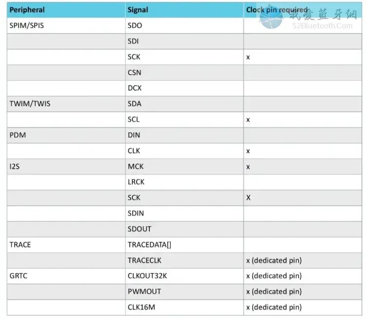
下图中红色GPIO口可用于时钟.
 image10.png.webp