马上注册,享用更多功能,让你轻松玩转社区。
您需要 登录 才可以下载或查看,没有账号?立即注册 
×
APPLICATIONS
• Televisions 2• 15-W/ch into an 8-�1�71�1�776�1�71�1�778 Loads at 10% THD+N
From a 16-V Supply • Consumer Audio Equipment
• 10-W/ch into 8-�1�71�1�776�1�71�1�778 Loads at 10% THD+N From a
DESCRIPTION 13-V Supply
• 30-W into a 4-�1�71�1�776�1�71�1�778 Mono Load at 10% THD+N The TPA3110D2 is a 15-W (per channel) efficient,
Class-D audio power amplifier for driving bridged-tied From a 16-V Supply
stereo speakers. Advanced EMI Suppression • 90% Efficient Class-D Operation Eliminates
Technology enables the use of inexpensive ferrite Need for Heat Sinks
bead filters at the outputs while meeting EMC
• Wide Supply Voltage Range Allows Operation requirements. SpeakerGuard™ speaker protection
from 8 V to 26 V circuitry includes an adjustable power limiter and a
DC detection circuit. The adjustable power limiter • Filter-Free Operation
allows the user to set a "virtual" voltage rail lower
• SpeakerGuard™ Speaker Protection Includes
than the chip supply to limit the amount of current
Adjustable Power Limiter plus DC Protection through the speaker. The DC detect circuit measures
• Flow Through Pin Out Facilitates Easy Board the frequency and amplitude of the PWM signal and
Layout shuts off the output stage if the input capacitors are
damaged or shorts exist on the inputs.
• Robust Pin-to-Pin Short Circuit Protection and
Thermal Protection with Auto Recovery Option The TPA3110D2 can drive stereo speakers as low as
4 �1�71�1�776�1�71�1�778. The high efficiency of the TPA3110D2, 90%, • Excellent THD+N / Pop-Free Performance
eliminates the need for an external heat sink when • Four Selectable, Fixed Gain Settings
playing music.
• Differential Inputs
The outputs are also fully protected against shorts to
GND, VCC, and output-to-output. The short-circuit
protection and thermal protection includes an
auto-recovery feature. 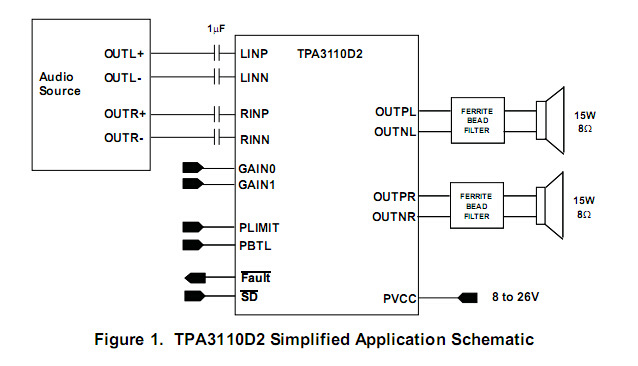
This integrated circuit can be damaged by ESD. Texas Instruments recommends that all integrated circuits be handled with
appropriate precautions. Failure to observe proper handling and installation procedures can cause damage.
ESD damage can range from subtle performance degradation to complete device failure. Precision integrated circuits may be more
susceptible to damage because very small parametric changes could cause the device not to meet its published specifications.
ABSOLUTE MAXIMUM RATINGS
over operating free-air temperature range (unless otherwise noted)
(1)
UNIT
VCC Supply voltage AVCC, PVCC –0.3 V to 30 V
SD, GAIN0, GAIN1, PBTL, FAULT –0.3 V to VCC + 0.3 V
VI Interface pin voltage PLIMIT –0.3 V to GVDD + 0.3 V
RINN, RINP, LINN, LINP –0.3 V to 6.3 V
Continuous total power dissipation See Dissipation Rating Table
TA Operating free-air temperature range –40°C to 85°C
TJ Operating junction temperature range(2)
–40°C to 150°C
Tstg Storage temperature range –65°C to 150°C
BTL: PVCC > 15 V 4.8
RL Minimum Load Resistance BTL: PVCC ≤ 15 V 3.2
PBTL 3.2
Human body model
(3)
(all pins) ±2 kV
ESD Electrostatic discharge
Charged-device model
(4)
(all pins) ±500 V
(1) Stresses beyond those listed under absolute maximum ratings may cause permanent damage to the device. These are stress ratings
only, and functional operations of the device at these or any other conditions beyond those indicated under recommended operating
conditions is not implied. Exposure to absolute-maximum-rated conditions for extended periods may affect device reliability.
(2) The TPA3110D2 incorporates an exposed thermal pad on the underside of the chip. This acts as a heatsink, and it must be connected
to a thermally dissipating plane for proper power dissipation. Failure to do so may result in the device going into thermal protection
shutdown. See TI Technical Briefs SLMA002 for more information about using the TSSOP thermal pad.
(3) In accordance with JEDEC Standard 22, Test Method A114-B.
(4) In accordance with JEDEC Standard 22, Test Method C101-A
DISSIPATION RATINGS
PACKAGE (1)
TA ≤ 25°C DERATING FACTOR (θJA) TA = 85°C θJP ΨJT
28 pin TSSOP (PWP) 4.48 W 27.87 °C/W 2.33 W 0.72 °C/W 0.45 °C/W
(1) For the most current package and ordering information, see the Package Option Addendum at the end of this document, or see the TI
website at www.ti.com.

PIN
I/O/P DESCRIPTION Pin NAME Number
Shutdown logic input for audio amp (LOW = outputs Hi-Z, HIGH = outputs
SD 1 I
enabled). TTL logic levels with compliance to AVCC.
Open drain output used to display short circuit or dc detect fault status. Voltage
compliant to AVCC. Short circuit faults can be set to auto-recovery by connecting
FAULT 2 O FAULT pin to SD pin. Otherwise, both short circuit faults and dc detect faults must
be reset by cycling PVCC.
LINP 3 I Positive audio input for left channel. Biased at 3V.
LINN 4 I Negative audio input for left channel. Biased at 3V.
GAIN0 5 I Gain select least significant bit. TTL logic levels with compliance to AVCC.
GAIN1 6 I Gain select most significant bit. TTL logic levels with compliance to AVCC.
AVCC 7 P Analog supply
AGND 8 Analog signal ground. Connect to the thermal pad.
High-side FET gate drive supply. Nominal voltage is 7V. Also should be used as
GVDD 9 O supply for PLIMIT function
Power limit level adjust. Connect a resistor divider from GVDD to GND to set
PLIMIT 10 I
power limit. Connect directly to GVDD for no power limit.
RINN 11 I Negative audio input for right channel. Biased at 3V.
RINP 12 I Positive audio input for right channel. Biased at 3V.
NC 13 Not connected
PBTL 14 I Parallel BTL mode switch
Power supply for right channel H-bridge. Right channel and left channel power
PVCCR 15 P supply inputs are connect internally.
Power supply for right channel H-bridge. Right channel and left channel power
PVCCR 16 P supply inputs are connect internally.
BSPR 17 I Bootstrap I/O for right channel, positive high-side FET.
OUTPR 18 O Class-D H-bridge positive output for right channel.
PGND 19 Power ground for the H-bridges.
OUTNR 20 O Class-D H-bridge negative output for right channel.
BSNR 21 I Bootstrap I/O for right channel, negative high-side FET.
BSNL 22 I Bootstrap I/O for left channel, negative high-side FET.
OUTNL 23 O Class-D H-bridge negative output for left channel.
PGND 24 Power ground for the H-bridges.
OUTPL 25 O Class-D H-bridge positive output for left channel.
BSPL 26 I Bootstrap I/O for left channel, positive high-side FET.
Power supply for left channel H-bridge. Right channel and left channel power
PVCCL 27 P supply inputs are connect internally.
Power supply for left channel H-bridge. Right channel and left channel power
PVCCL 28 P supply inputs are connect internally.
FUNCTIONAL BLOCK DIAGRAM 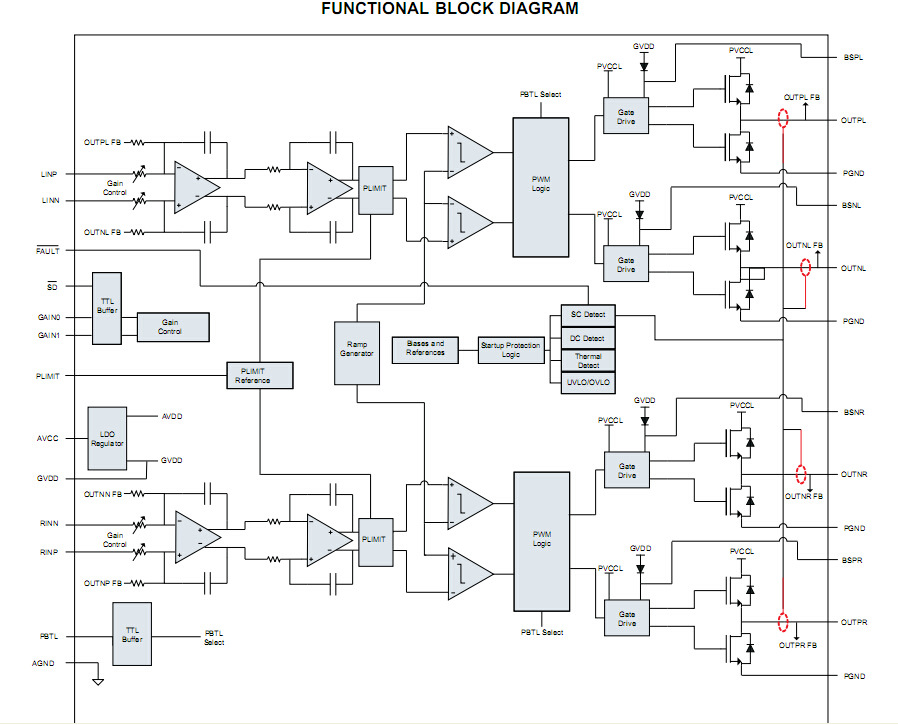
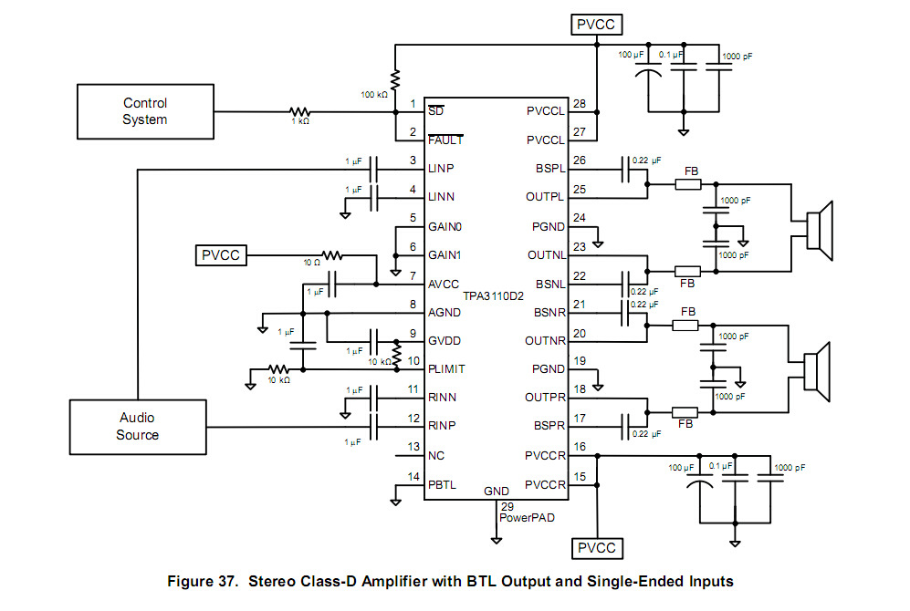
APPLICATION INFORMATION
如果您有功放IC、蓝牙模块、音频解码模组、苹果周边设备方案解决及其他软件方案解决需要话,请与我们联系,我们会为您提供样板和报价。谢谢!
电 话: 86 0755 27491316-8031
移动电话: 18898795323
| 
 发表于 2015-4-22 11:10:27
 提升卡
提升卡 置顶卡
置顶卡 变色卡
变色卡